Search Results
7/2/2025, 11:25:20 AM
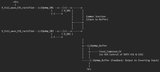
Part B: Active OR Gate (Precision Maximum Selector)
(Takes inputs from the outputs of the two PFWRs)
Explanation of Active OR Gate (Part B):
1. Inputs (V_full_wave_CH1_rectified, V_full_wave_CH2_rectified): These are the already full-wave rectified and active outputs from the two channels.
2. OpAmp_OR1 / D_OR1 and OpAmp_OR2 / D_OR2: These two branches form the core of the precision OR gate.
Each op-amp (OpAmp_OR1, OpAmp_OR2) is configured to act as a "super diode" for its respective input and associated diode (D_OR1, D_OR2).
The op-amp will drive its output such that the voltage at the cathode of its diode (the Common Junction) precisely matches its input voltage (V_full_wave_CH1_rectified or V_full_wave_CH2_rectified), effectively compensating for the forward voltage drop of D_OR1 or D_OR2.
3. OR Logic: As explained previously, because the op-amps actively compensate for the diode drop, the Common Junction will always rise to the voltage of the highest input (MAX(V_full_wave_CH1_rectified, V_full_wave_CH2_rectified)). The diode connected to the lower voltage will be reverse-biased, isolating its respective op-amp.
4. OpAmp_Buffer: This final op-amp is a simple voltage follower. It takes the highly accurate, but still somewhat high-impedance, Common Junction voltage as its input. It then provides an extremely low-impedance output (Final_Combined_CV) to drive the VCA control inputs of both channels reliably, without loading down the precision OR gate.
Page 1