Anonymous
(ID: LFsKt2k3)
 7/13/2025, 3:40:44 PM
No.510265934
>>510266506
>>510268212
>>510268249
>>510268535
>>510268838
>>510269252
>>510269375
>>510269954
>>510270047
>>510270259
>>510270319
>>510270421
>>510270493
>>510270820
>>510270943
>>510271504
>>510271747
>>510272057
>>510272736
>>510273374
>>510274624
>>510274791
>>510274816
>>510275876
>>510276087
>>510276178
>>510276410
>>510278235
>>510278491
>>510279293
>>510279836
>>510279872
>>510279902
>>510280122
>>510280764
>>510281546
>>510281755
>>510281906
>>510282319
>>510282783
>>510283186
7/13/2025, 3:40:44 PM
No.510265934
>>510266506
>>510268212
>>510268249
>>510268535
>>510268838
>>510269252
>>510269375
>>510269954
>>510270047
>>510270259
>>510270319
>>510270421
>>510270493
>>510270820
>>510270943
>>510271504
>>510271747
>>510272057
>>510272736
>>510273374
>>510274624
>>510274791
>>510274816
>>510275876
>>510276087
>>510276178
>>510276410
>>510278235
>>510278491
>>510279293
>>510279836
>>510279872
>>510279902
>>510280122
>>510280764
>>510281546
>>510281755
>>510281906
>>510282319
>>510282783
>>510283186
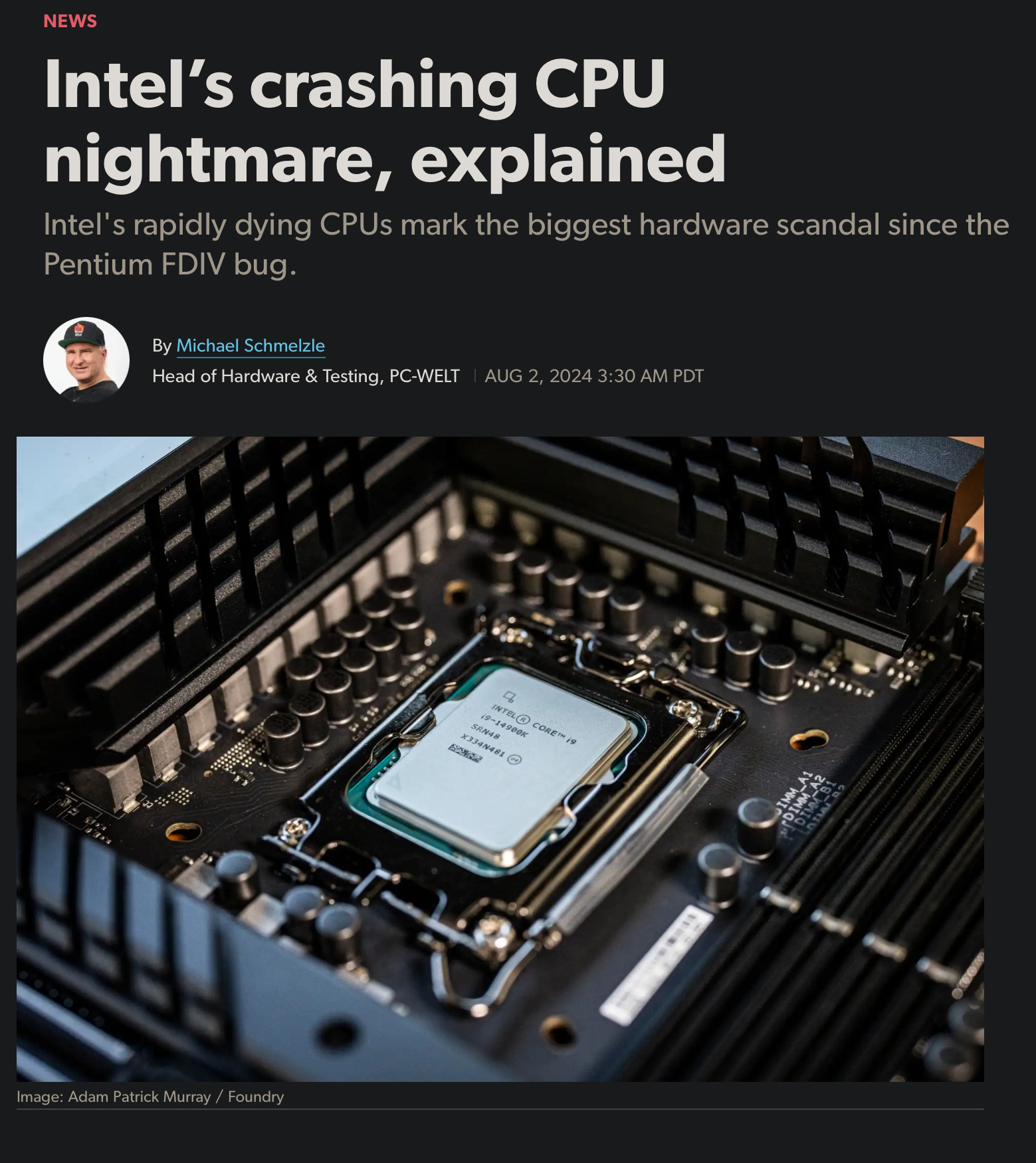
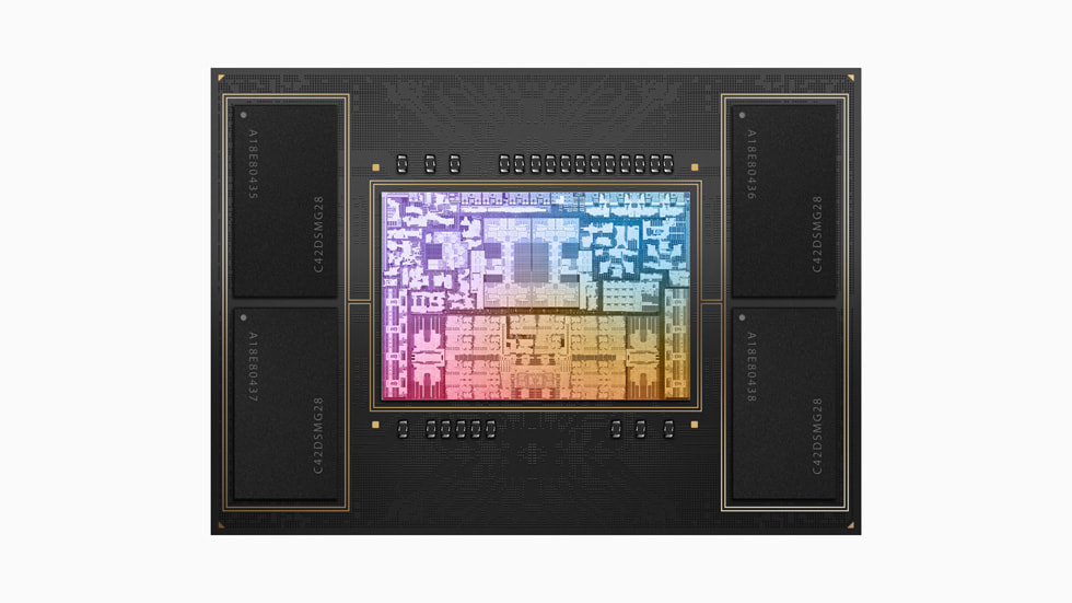
Why can’t we produce chips?
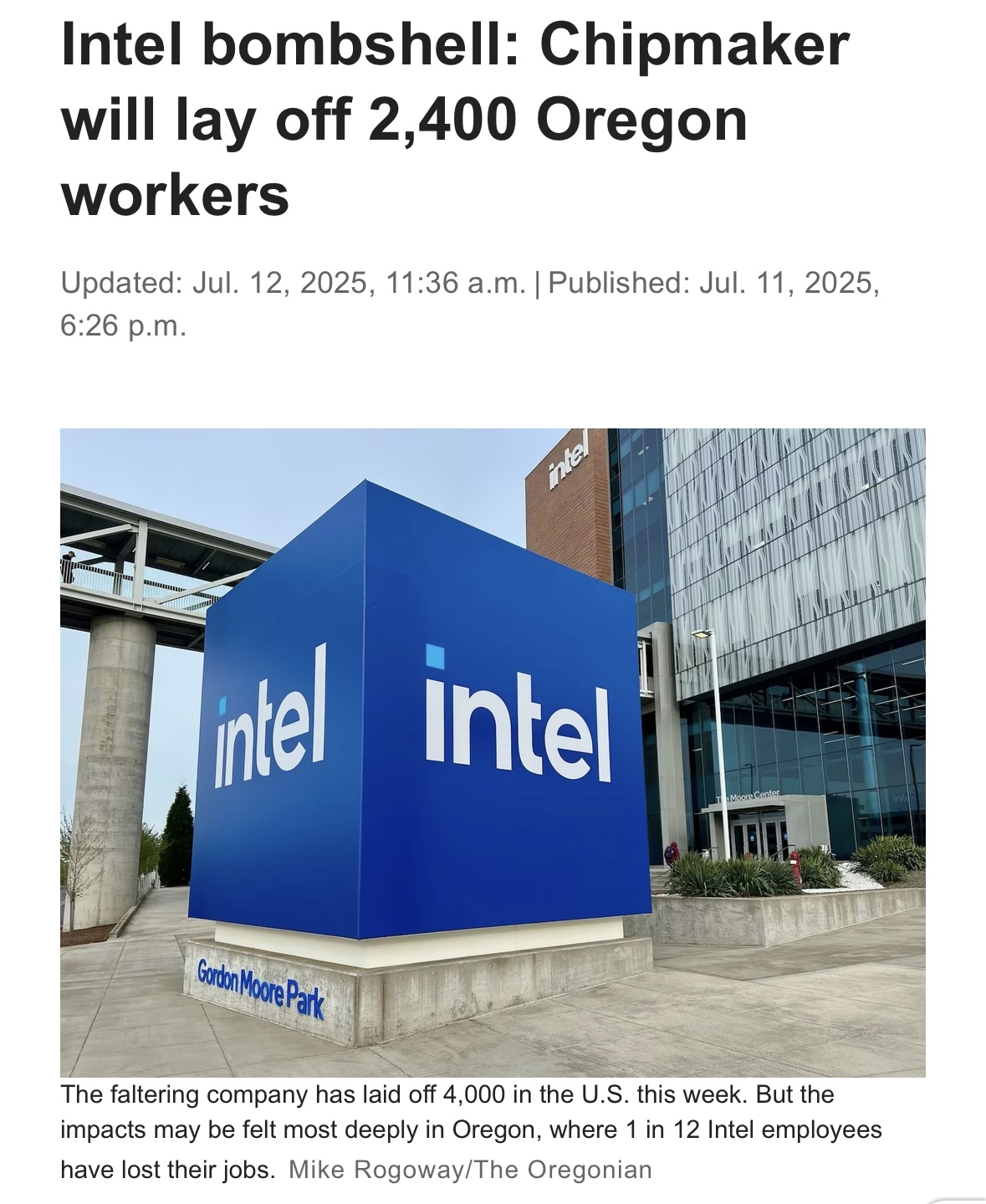
Literally all of the planned fabs are being cancelled.