Search Results
6/16/2025, 6:08:02 AM
>>2924312
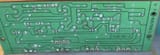
Your design is wrongly conceptualizing the problem as conductive interconnecting traces.
I, too, was on that level at one point, early in my career. Don’t worry, though. It’s a phase and you’ll overcome it.
Eventually I realized the problem was to start off with everything connected (the initial copper layer before etching) and add the absolute minimum amount of insulating gaps in the right places on the copper layer to enable the circuit to function.
6/16/2025, 5:57:18 AM
>>2924312
You’re design is wrongly conceptualizing the problem as conductive interconnecting traces.
I, too, was on that level at one point, early in my career. Don’t worry, though. It’s a phase and you’ll overcome it.
Eventually I realized the problem was to start off with everything connected (the initial copper layer before etching) and add the absolute minimum amount of insulating gaps in the right places on the copper layer to enable the circuit to function.
Page 1