Search Results
7/15/2025, 5:25:28 PM
>>715511105
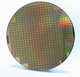
From 1970 to 2010, this thing, a wafer had basically a fixed price of $4000.
Every 18 months give or take, we would improve the resolution of the UV projection, and double the number of components you can put per square mm, and the price would still be $4000 (this is the so called moore's law)
However we got to a point where this stopped working, not because we can't go any smaller, but because circuits stop working due quantum tunneling shit. electrons will just teleport around like son goku on crack.
Now what we get instead is the industry just refining the components, making pieces that do more complex tasks, making more layers on the chips that require more manufacturing steps,and as a result, the wafer price is going up.
It's according to this newspiece, it's $18000 for the 3nm wafer:
https://www.tomshardware.com/tech-industry/tsmcs-wafer-pricing-now-usd18-000-for-a-3nm-wafer-increased-by-over-3x-in-10-years-analyst
This means that we're under the jensen's law now (if you want more transistors, you pay more, if you want low power transistors, you pay even more).
There are ways to alleviate this such as chiplets or just piling up ICs which is how the switch 2 has that memory bandwidth, but sadly you have to forget this mentality you could rely on your entire life.
And there's not even some hibernian conspiracy behind it, it's just quantum physics being annoying. (also it's the same phenomena we use to make SSDs)
6/15/2025, 12:08:59 AM
>>712672139
It's just not the coof, the moore's law is over.
From 1970 to 2010, we could just make the entire circuit of a chip smaller by improving the lens and making the mask bigger or with a higher resolution.
It was a constant $4000 per wafer, and every 18 months give or take, you could shove twice the number of components in the same die.
But we got to a point where the smaller shit like the tracks fail to work normally if you shrink em down. quantum tunneling makes electrons teleport around like crazy. we do abuse quantum tunneling to make flash memory, but in this case is undesirable and unavoidable.
What replaced it is what i call "the jensen's law". Instead of shrinking down EVERYTHING, we now re-design the components to use less space. the end result of this is that we both burn billions in research, and need more manufacturing steps to do a wafer, and as the end result, the best the manufacturing step, the more expensive is the wafer.
3nm is 18000$ according to this article:
https://www.tomshardware.com/tech-industry/tsmcs-wafer-pricing-now-usd18-000-for-a-3nm-wafer-increased-by-over-3x-in-10-years-analyst
It's what is being used on the PS5 pro, which is why it costs $700.
Page 1