>>712669235
Unicorn Overlord.
Emmm Astro Bot
Death Stranding 2 but thats gonna come to PC in a year?
Demon Souls Remake
GTA 6 I guess but thats also on the PC in a year
>>712675008
It was and I don't undersatand what these people need to do to get fired by the Japanese masters. They released that the PS5 made a total of 15 billion in profit. Now I don't know if that counts the losses or not.
But they're basically 99.5% dependent for profit on 3rd parties and thats a massive loss for them in terms of potential revenue.
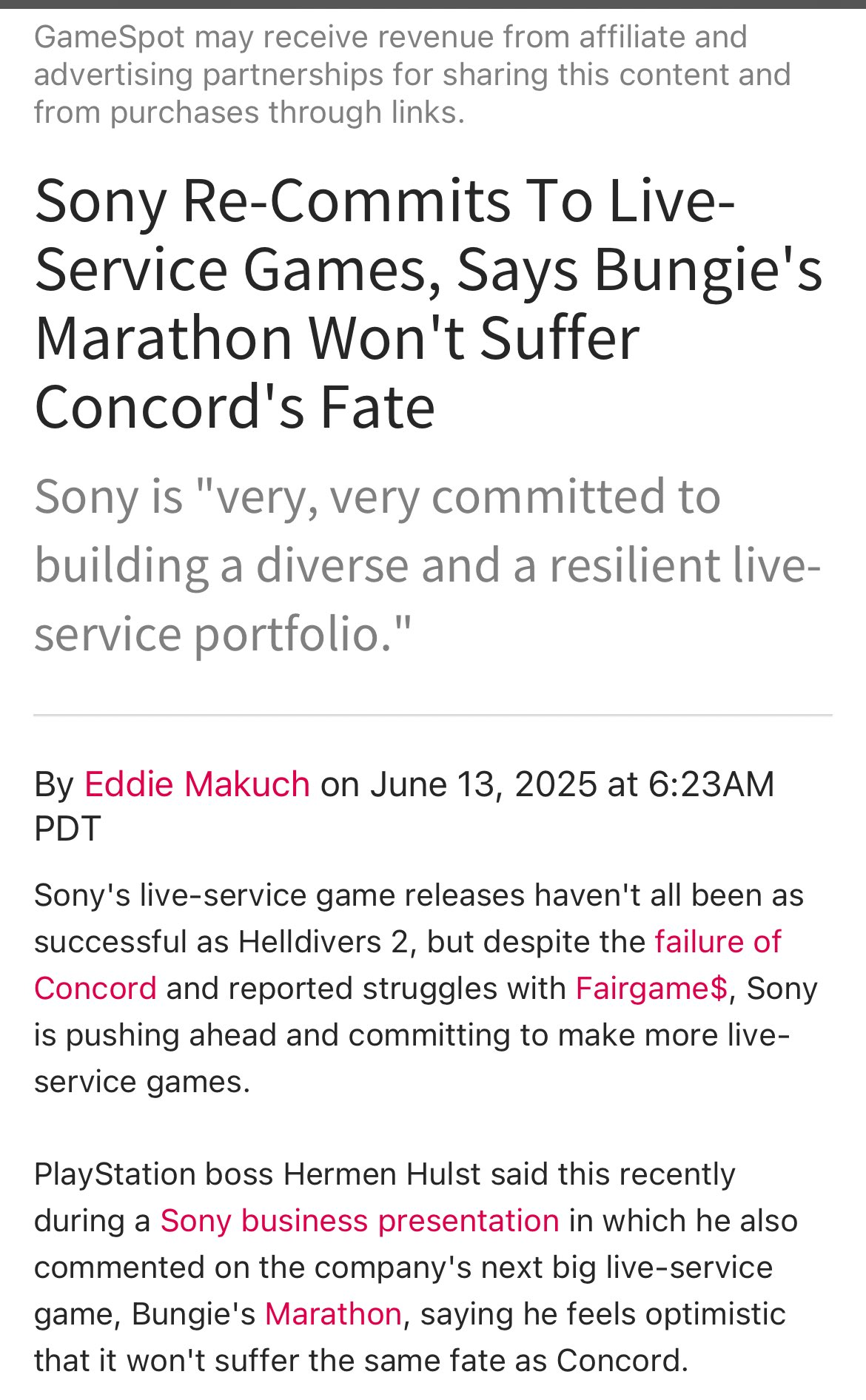
Whats even more confusing to me is that Concord lost them about 500 million dollars.
Fairgames and Marathon is going to cost them another 500 million dollars and thats not even counting their $3.6bn waste on buying Bungee that most certainly did not make that money back in Destiny sales.
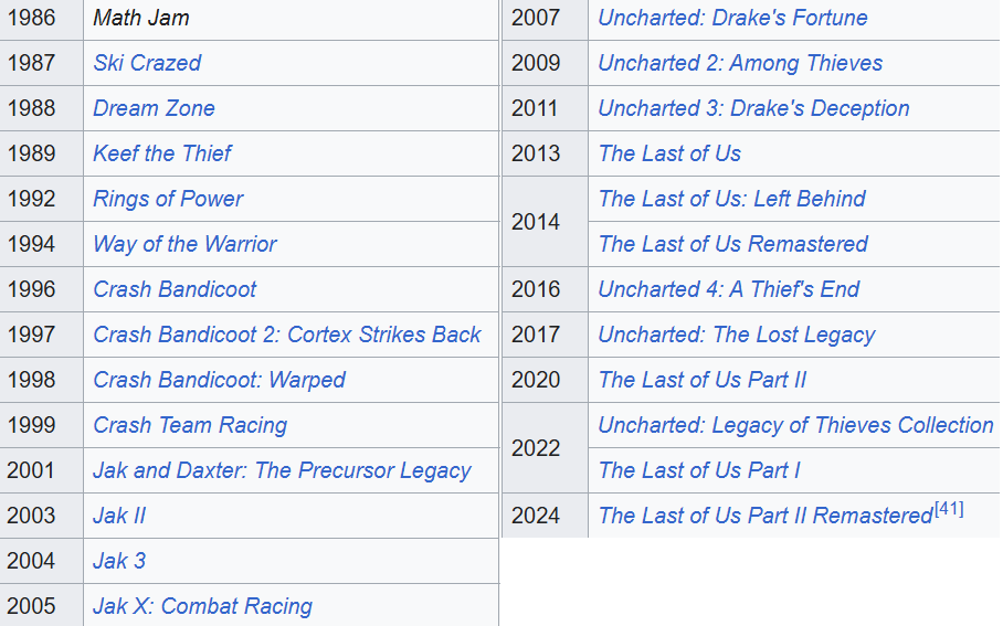
So they made 15 billion dollars of profit but lost 5 billion on just 3 things. They also lost ??? on Naughty Dogs shitty game. The let Neil Fuckman basically kill Naughty Dog. They released 0 new IPs and they explanded 0 of their existing IPs with God of War and Horizon Zero being basically forgoten by everyone not meeting their sales expectations.
On the way they have Ghost of Yotai that is probably going to underpreform as well.
So after all these CATASTROPHIC decisions. Why is Sony Americas Leadership even employed at this point? Are they taking credit for all the 3rd parties being on the PS5? Are they taking credit for designing the PS5 basically a cheap PC with no real features that set it apart for Xbox?
Like what the fuck is happening? Why aren't heads rolling left right and center?